Saturday, November 28, 2015

Non Contact Temperature Measurement using MLX90614         

               
                   IR thermography is the one of the concept ,that is used for monitoring temperature value without attach on the substance .So it is having more advantageous .By using MLX90614,we can monitoring oil, fruits and food temperature also .Here I have attached one of my prototype concept while working on it.


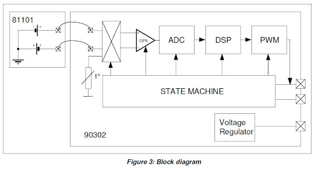
Functional diagram:

       The sensor is having inbuilt DSP FIR filter algorithm.So output of the sensor is very stable and good accuracy .But based on the distance the accuracy will be changed.And then it supports SMBus protocol. SMBus protocol seems to be same as I2C protocol but clock rate varied.

If you know about SMBus, go through the following site


Step 1: Check it out device address for MLX90614


Device address with write  - 0xB4
Device address with read   - 0xB5

Device address without read and write bit -0x5A


Step 2: Check it out fclk or sclk


Step 3: Voltage rating


Step 4: Write down the driver code as per the following clock and protocol format


Step 5: Write down the application layer


Step 6: Calibration and data conversion code


Step 7: Testing your code

You can get my sample code from my github account.


While monitoring on the cooling water battle


While monitoring on the boiled egg


Friday, November 27, 2015

         Getting started with RTOS for Low End MCU
           At my earlier stage, I started with RTOS application, that time I got so much confusion .Because of that time, I was hearing about the lot of RTOS names (Vxworks, FreeRTOS, RTLinux ,Windows Embedded and so on).So I got confusion. Because how I am going to start with, and which one is suitable for my microcontroller. I don’t know clearly.
           Finally I got it the Salvo RTOS by thegoogle on the net and also great introduction about RTOS from my teacher Mr.Christy Mano Raj,Assistant Professor at Government College of Engineering, Salem. These RTOSsuitable for 8051 architecture based controller and also other lower end architecture microcontrollers. So I can easy to start my own RTOS application. But depend on the reliability, you can choose other RTOS. But the fundamental of the RTOS is common. So this RTOS very suitable for startup peoples. And another specialty is that, it can support 8051 MCU series and PIC 16F series BSP support. That means, if the guys who have knowledge on 8051 and PIC 16F series, they can able to start RTOS. So we don’t feel about 16 bit or 32 bit architecture controllers.
         The following link redirected you to getting details about the list of the micro controllers those are supported by SALVO.
           Here I am sharing one of my experience, when I started my RTOS development.
What is meant by RTOS and Kernel?
            The operating system (OS) contains the kernel, the timer and the remaining software (called services) to handle tasks and events (e.g. task creation, signaling of an event). One chooses a real-time operating system (RTOS) when certain operations are critical and must be completed correctly and within a certain amount of time. An RTOS-enabled application or program is the end product of combining your tasks, ISRs, data structures, etc, with an RTOS to form single program.
Reference : Salvo User Manual
First of all you have to know the following details (RTOS fundamental tools),
1) Task states
2) Tasks
3) Multitasking
4) Scheduling and types of the scheduling
        a) Round robin scheduling
        b) Preemtive scheduling
 5) Inter task communication tools
         a) Message
         b) Queues
         c) Event flags
 6) Deadlock
 7) Priority inversion
          Here I have added a web link. By the way, you can download the Salvo RTOS user manual.
          It contains that full details about RTOS fundamentals (See Chapter 2, Page No:11). These fundamentals are common for the all kind of RTOS. All of them having same characteristics.But the declaration and structure only different .
For example,
The task declaration for Salvo is,
OSCreateTask(TaskA, OSTCBP(1), 10);
 But the task declaration for FreeRTOS is,
// Create the task, storing the handle.
xTaskCreate( vTaskCode, "NAME", STACK_SIZE, &ucParameterToPass, tskIDLE_PRIORITY,&xHandle );
         The above both statements are given as eligible(Salvo) or ready(FreeRTOS) to the corresponding task.So that kernel is able to running the corresponding task.

Salvo RTOS Task  State


FreeRTOS Task State

you can download my code through my github account:
https://github.com/msuresh168
Recently i have attached the following codes,
1.Multitasking for 8051 MCU using Salvo RTOS
2.LEDBlinking_AtMega128 by using FreeRTOS (Same way Multitasking concept)

Friday, July 31, 2015

I2C Bus extender


     Sometimes I feel to communicate my data for long distance via an I2C bus communication. But unfortunately the I2C protocol supports very few meters only. As a normal application interfacing such as RTC, external memory or I/O extender doesn’t need a long distance for communication. Here the slave and master can be placed closely on those applications.
        But when we are going to use special functions ( interfacing with AFE, Motor driver IC and etc.), we have to carry our I2C signals for the long distance. Because of our master communicate with slave remotely, not a board itself.
        Here I have attached one of my sample schematic diagram .I have tested this circuit one of my application. I have used P82B715 (TI manufacture).This IC can communicate up to 50 meters without any data losses.
      For a very long distance communication, you can use following formula (figure (a)) to find out pull resistor values otherwise go through their manufacture datasheet. But anyway 4k7 and 470R suitable for most of the applications (figure(b))

figure(a)


                                                  figure(b)

Have your PCB design isolated between AGND and DGND?


    Generally AGND, DGND stands for Analog and Digital Ground respectively. Recently most of the microcontrollers and AFE (Analog Frond End) chips are having separate ground pins (consists of AGND and DGND separately).

     
    Because of an Analog signal can be easily affected by a noise signal, which has been produced by a digital signal related components (ie... relay switching, solid state devices, motor driver and etc.).So we have to beware about PCB layout designing side.


    The figure (b)  is showing, how the ADC signal affected by the noise signal. Actually when we are consider about the digital signal, the MCU is having min and max threshold limit value by their manufacture for input signal processing. So we don’t care about digital signal consideration. But the ADC signal continuously has been taken when the ADC sampling processing time (figure(b)).So your noise signal also may be sampled at that time. It leads to take you observe wrong ADC values.


For Digital signals consideration (figure (a)),

0 to 1.5 -0 voltage that means ‘1.5 Volts’ –min threshold voltage level.
3.5 to 5 -5 voltage that means ‘3.5 Volts’ -max threshold voltage levels.

Note: min and max threshold voltage level may be varied from one MCU to another MCU. Here I have taken that values are approximately.

Here we can get only 0V or 5V .So the noise signal has never affect the digital signal.

For Analog signals consideration (figure (b)),
0 to 5 –it have collective of range (steps resolution).So we have to think about noise signal. It may affect our original ADC signal.

                                                                figure(a)


                                          figure(b)


We can reduce our noise level by the following ways,
  1. Separate your AGND and DGND plane area in CPU and all add-on boards(ie.. even ADC or motor driver board also) as a figure (c).                                                                                             
  2. Moreover trying to use individual power supply for all add-on boards (should be isolated ground) and finally connected together with all the ground pins (if needed) using star ground technique.                                                                                          
  3. Always kept away your filter circuit and analog related components from your Motor driver or any solid state related components.                                                                                              
  4. Place your sensor, Amplifier and AFE (Analog Front End)ADC chips very closely .If the length of wire or track on the PCB may increase ,you may lose few micro volts .(For 18 bits resolution ,each and every bit can be changed by 15.625uV at 2.5V Ref. So you have to create the best PCB trace for ADC higher bits resolutions).                                                                                                
  5. The isolator IC which can prevent your components as well as reduce the noise level.

Here I gave few isolator ICs details with suitable application,

GPIO –ISO7340
SPI    –ISO7341
I2C    – ISO1540
PWM – ISO7821

The isolator IC can be used by the following three ways,

a) Level swifter (5 to 3.3V or vice versa)
b) Protect the pins from reverse current or any other fault condition
c) Isolate the ground signal from the noise signal

Note: Here I have just consider about TI chips only. But most of the companies, they are designing the same type of isolator chip with different type of the parameters. So let’s consider about it.


 If your design satisfies the above conditions, you can able to get the best accuracy results and protect your ICs from unwanted signals.

figure(C)

  
                                                         figure(d)

Is your design having Anti-aliasing filter at that time of ADC sampling?


          Anti-aliasing filter which is going to be used for remove a higher frequency noise signal before to be taken a sampling processing at that time. Generally the sampling frequency should meet with Nyquist theorem .But in this case, the Aliasing signal doesn’t satisfy with Nyquist theorem. So that, your ADC digital values may be fluctuated that means aliasing happened.  

Nyquist Theorem:
(ADC) fs >= 2 x fc
     The maximum frequency of the input signal is less than half or equal to sampling rate (fs).

For example, if you are application having the frequency of the sensor signal is 1KHz, you can choose your cut off frequency of anti-aliasing filter is greater than 1KHz and it should be less than sampling rate of your ADC. Here my sampling rate for my ADC is 10KHz so that I have designed my cut off frequency of my filter is 5KHz.

Here I have chosen cut-off frequency (fc) (input signal frequency) is half of my ADC sampling rate (fs).


The following online design tool may helpful for you.
Recently I have used ST electronics android application. It’s really very fun.
You can go through the following link to work for OpAmp circuit and filter design,

Digital filter:
     This is one of the algorithm technique .Generally we are displaying ADC digital value for every sampling processing. But here we can display the average of 20 or 30 (whatever..) digital values. So we can avoid fluctuated data.
The algorithm looks like this,
 Total=ADCValue=FinalVlaue=0;
for(int i =0;i<=20;i++)
{
ADCValue=ADCRead(channel); 
Total=ADCValue+Total;
}
FinalValue=Total/20;
SAC Vs Delta Sigma:
Here I don’t discuss about SAC and Delta Sigma architecture. So we will see again in my future tutorial. But right now I will try to explain about differences and few valid points for our application. Last one year I was using Delta Sigma Architecture ADC. Because it suitable for my following application.
1. It is very accuracy .We don’t feel about Anti-aliasing filter at all. But depends on your application you may need filter circuit.  
2. Compare with SAC architecture, it have slow speed. But it does almost reach enough speed.
Both AFD type ADC chips have I2C and SPI protocol communications.
1. ADS1231:
2. MX7705:
3. MCP3421:


Star Ground System


                  It is one of the essential concept for the system designer .By which, we can limit the noise level for our system. When the people, who are going to interfacing with lot of the boards in the single system, they got ground noise signal. Generally this noise signal induced by the solid state relay, switching application or any other motor driver. But a digital signal is never affected by the any ground noise. But an analog signal is getting affected easily. When you are going to take ADC signal about the sampling voltage level mV or uV, you may get noise values.

You can reduce ground noise following ways,


             1. In case your system is having 3 more boards, the power supply for the three boards should be connected with SMPS terminal directly.


         2. In case the first rule not possible, just create a small intermediate stage from SMPS to hub(just kind of small board to distribute power supply). After that all the boards connected with hub's ground directly.